TSMC demonstrates readiness for 3D-IC
One of the more interesting things about 3D-IC is how much of it is about scaling up – about as counter-intuitive a phrase as you can get in silicon design. Though obvious when you think about what we want to cram into these packages
To understand that, it’s worth taking a look inside the pathfinder work underway at TSMC. It aims both to demonstrate capability to customers and so that the foundry itself can test, validate and verify the 3D-IC technologies.
Jerry Tzou, the company’s deputy director – Backend Business Division, provided a quick tour through the demonstration projects at last week’s GSA Memory+ conference in Taipei, Taiwan.
CoWoS interposer development
TSMC has interposer product shipping in volume with Xilinx already, but this is only the beginning. Tzou walked through four different demonstration projects in hand for its CoWoS (Chip-on-Wafer-on-Substrate) technology. But first, what are some of the general challenges.
At a basic level, Tzou identified six:
- Testing of the passive interposer
- Inter-die LVS/DRC
- Microbump assignment and RDL routing
- RC extraction
- Thermal analysis
- Inter-die interconnect test
Now let’s look at the interposer projects themselves.
1. Integration of three dice on an interposer
This project addressed all the issues above, and involved bringing together three different functions also at different nodes. Specifically, these are a 28nm logic die, a 40nm eDRAM and a 65nm GPS chip.
These were all TSMC dice and a key objective was therefore to verify the methodology and inform last month’s release of an updated Reference Flow for 3D-IC.
2. Integration including third-party Wide I/O DRAM
One of the realities about both vertical and horizontal integration is that there will be silicon and technology to incorporate from multiple sources.
“Third-party die creates a new set of challenges,” Tzou said. “How do we work with the third-party to make sure their material is compaitible with us, with our processes, with our technology without any issues.”
This feeds into the critical yield issues that apply to 3D-IC, what Tzou identified as “the name of the game”. This particularly applies where more advanced designs and chips will be part of the integration.
In this demonstrator, TSMC integrated three elements and this time it focused on 40nm devices. These were:
- TSMC logic (40nm)
- TSMC eDRAM (40nm – 1GHz/1024bits, 128GB/s)
- Third-party WIO DRAM (200MHz/512bit, 12.8 GB/s)
3. Integration of high-bandwidth memory
This took entirely third-party technology and integrated it as a daisy chain on a full reticle size 26mm x 32mm test vehicle. Of course, size here matters. The more dice you can get on the interposer, the greater advantage you can take of the performance boost offered by proximity positioning of about 30um side-by-side.
This demonstrator looked to address the demands of mobile computing and requirements for both app and graphics processing, but it also points the general direction. And in that regard leads perfectly into the fourth interposer project.
4. Extra large interposer
“People want to make the best of the real estate,” Tzou said. “They want to get as many die as possible to increase performance or functionality. A bigger interposer means they can put more on there.”
This project delivered an interposer of 26mm x 48mm (now at 1.5X of the reticle size) on a package substrate of up to 60mm x 60mm. Tzou offered a diagram of where this next step could boost interposer-based integration.
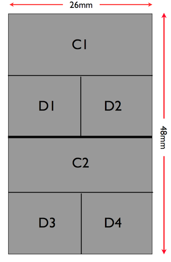
Mapping an Extra Large Interposer (Source: TSMC)
Tzou also previewed TSMC’s InFO wafer level package. InFO is short for integrated fan-out and the idea is to take the interposer concept and transport it across in a cheaper and less dense form to still more potential 3D-IC applications.
Right now, it has been validated – largely in single die format – for sizes of 8mm x 8mm and 15mm x 15mm, but the commercial target is to bring this to a genuine multi-die 25mm x 25mm size next year. InFO’s maturation path looks like this.
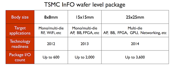
TSMC InFO objectives (Source: TSMC)
Full 3D-IC demonstrator and updated TSMC roadmap
Finally, Tzou showed a demonstrator for the stacking of a DRAM cube on 28nm logic, again aimed at mobile applications. This has been used to characterize TSV design rules through the test and functional verification of a customer test vehicle.
Combined with the interposer work, TSMC’s updated 3D-IC roadmap therefore now looks like this.
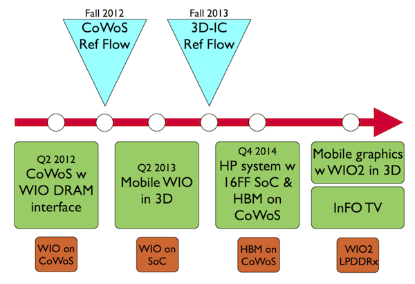
Updated TSMC 3D-IC roadmap (Source: TSMC)
This is very much a confidence building exercise, and it is going on across the industry right now, certainly among IP, design services, EDA and foundry players. And it has to – and right now, there’s enough meat in there to see it working.
