Amkor keeps question mark next to ‘full’ 3D-IC in 2016
3D-IC projects today are on yields of at best between 95% and 96%, according to leading packaging player Amkor Technology. The market is looking – as it always does – for ‘three nines’.
Dr Choon-Heung Lee, Corporate Technology Officer, told the GSA Memory+ Conference in Taipei, Taiwan that the main holdback is middle-end-of-line (MEOL) processes.
This the first block of MEOL processes he brought to his audience’s attention.
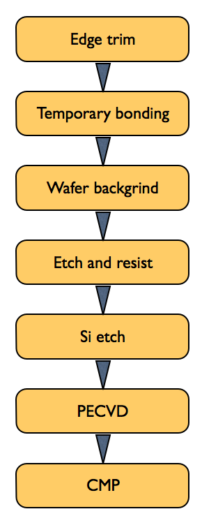
3D-IC MEOL steps, stage one (Source: Amkor Technology)
However, this is followed by a second stage culminating in die separation and visual inspection.
“Don’t expect 99.9%,” Dr Lee said, noting that while other stages are at or around this level, the final yield is calculated by multiplying together all five steps involved aside from MEOL through to test. In order the stages are:
- Front-side bumping
- MEOL
- Back-side bumping
- Assembly
- Test
Dr Lee cited the 95-96% yield figure for “four FPGAs side-by-side”, referencing the market that has led the way in adopting heterogeneous interposer-based 3D-IC technology.
In many respects, Amkor and others are making statements like these as much to manage expectations over 3D-IC’s adoption across various markets. “We are ready,” Dr Lee said, echoing the general claim from silicon infrastructure providers.
As heterogeneous FPGA projects will initially focus at the higher end – exploiting interposer’s current availability as well as performance, cost and manufacturability advantages – so a ‘sub-optimal’ yield for those markets could be very profitable.
As Dr Lee noted, the key to adoption has to be, “Is there any reasonable return.” Though he then more jokingly added. “As my CEO asks, ‘Hey, I’ve spend $40m on 3D. Where’s my return?'”
Still more pointedly, he offered a very general roadmap for the adoption of 3D-IC technologies, including a contrast between the mobile apps-processor-plus-memory model that is pushing the consumer OEMs towards through silicon vias and those with broader high-performance requirements.
Noting that Samsung is pushing to have TSVs in products at the 14nm node next year, he again noted that such goals are for “introductory technologies”. At the mobile level, Amkor gives ‘full’ stacked 3D for consumer a 2016 date for broader adoption.
And even then, it is couched with a question mark.
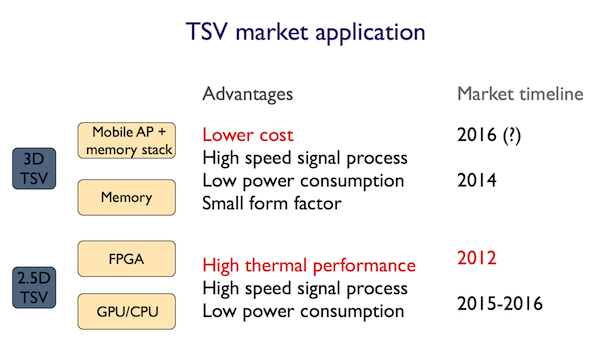
Amkor 3D-IC adoption roadmap (Source: Amkor Technology)
