India outlines subsidies for foundry fab plan
The Indian government says that it is prepared to meet up to 25% of the cost of developing a 45nm foundry and provide further incentives to support the growth of the national electronics manufacturing, according to a preliminary tender published this week.
The fab must have capacity to run 40,000 starts per month on 300mm wafers, and also service designs aimed at the 90nm and 65nm nodes. It may also only use second-hand fab equipment for ‘non-critical’ functions.
Alongside tax incentives, a further 25% subsidy may also be available for ‘growth capital expenditure’. This may refer to a broad target to introduce 28/22/20nm production within two years of ‘the initial phase’.
The project is overseen by the Department of Electronics and Information Technology (DEITY).
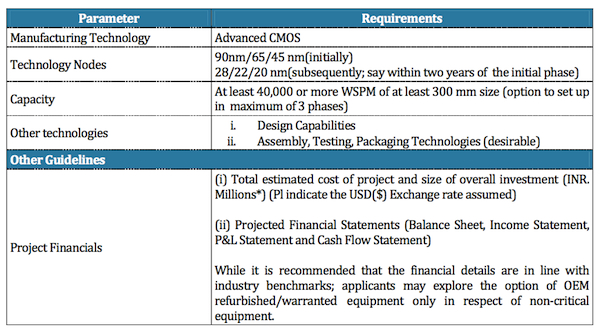
India’s wafer fab goals (Source: DEITY)
Two groups have so far tabled Indian fab proposals. One is made up of IBM, Israel’s Tower Jazz and local company Jaiprakash Associates. The other has STMicroelectronics, Silterra and local partner Hindustan Semiconductor Manufacturing Company as members. Both projects have a value of about $4bn.
Overall, DEITY believes that India will need to build 15 foundries of varying sizes, although this sounds very ambitious given current global capacity and the possible further growth in output that 450mm wafers could bring. Then there are China’s ambitions to grow its foundry sector.
Foundry plan context
Wafer fabs were raised as part of India’s National Policy on Electronics (NPE), published last year. This has the aggressive overall aim of bringing the turnover of the local market to $400bn by 2020, with some $55bn of that generated by chip and embedded software design. The foundry’s sales would be in addition to that last target.
India has long wanted to build its own ‘soup-to-nuts’ electronics systems business, cutting out the export of manufacturing, packaging and test work to elsewhere in Asia since its design sector began to mushroom.
At first glance, the DEITY targets take India along the wafer fab technology curve at a comparatively conservative rate – although the government’s exposure would be comfortably in the multibillion-dollar range given its targets and conditions. India anticipates that private and public sector investment required to reach the NPE’s goals will be approximately $100bn.
The fact that the initial foundry plan does not target what would be a leading edge process node from the foundry’s opening day is not necessarily that big a disadvantage in servicing growing domestic demand.
India’s design services sector does target some work at 28nm and is preparing for 20nm. However, domestic fabless companies and those who supply third-party design are typically working on implementations for older processes.
A bigger question may be the export regime that applies from India for finished silicon. Apart from their technological might, the big players such as TSMC, Samsung, GlobalFoundries and IBM have their facilities predominantly in countries with liberal export regimes. India has long been considered more problematic, even than China, and there is the ever-present question of corruption.
The Expression of Interest is seeking initial responses by 6 November, 2013, a little under a month from now.
