Oxygen injection for go-faster 14nm transistors
At this year’s IEDM, researchers from Mears Technologies and the University of California at Berkeley are reporting on their modelling work on a technique they believe could be more effective than strain at the 14nm node.
Robert Mears, founder of Mears Technologies, presented the idea of using a ‘superlattice’ structure to break up the silicon channel – in this case on a silicon-on-insulator (SOI) transistor – at the 2007 SOI Conference. That paper did not go into detail into how the superlattice for the Mears MST device was formed but the central idea was that insertions into the silicon lattice would break up periodicity in the vertical direction but maintain the band structure horizontally. This would have the effect of reducing scattering: increasing the effective mass of carriers moving vertically but reducing it in the direction of transport. Mears termed the material MST-SOI.
The element that UC Berkeley and Mears have been working with to act as the lattice breaker is oxygen. At IEDM, the team is presenting modelling work based on the idea not just for SOI devices but for bulk CMOS as well, testing their predictions with a Poisson-Schrödinger solver against experimental transistors.
The superlattice growth technique, which has not changed significantly since 2007, uses a standard CVD epitaxial reactor rather than something more exotic, such as atomic layer deposition.
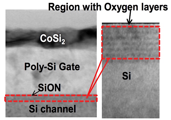
Pictured Cross-section of Mears/UC Berkeley transistor with superlattice section highlighted
The researchers argue that the simulations show that the superlattice structure forces electrons into sub-band valleys that have a lower transport mass, which increases mobility. Gate leakage also drops as the tunnelling effective mass goes up. Electron mobility is still helped by the use of strained silicon but as the two methods overlap in their effect, you get a diminishing return on using both. The technique would let chipmakers trade one off against the other and the researchers believe that oxygen insertion offers better bang for your buck than strain on n-channel MOSFETs and about the same performance on p-channel devices.
They add: “For both electrons and holes, the combination of strain and oxygen-inserted layer yields the highest mobility.”
The team performed simulations on FD-SOI and finFET devices as well. FD-SOI might gain more from oxygen insertion because it is harder to strain than the finFET. But, because the technique also serves to confine the inversion layer through which the carriers move when the device is switched on, gate control improves which should be good news from a drain-induced barrier lowering (DIBL) point of view.
