FinFET tipsheet for IEDM
 Dr David M Fried is Chief Technology Officer - Semiconductor at Coventor, responsible for the company’s strategic direction and implementation of its SEMulator3D Virtual Fabrication Platform.
 At the upcoming IEDM, we’re likely to see a great deal of discussion about finFETs (Guide). Many groups are pursuing the goal of fully integrated finFET CMOS technology using a variety of approaches that have some similarities, but many key differences. Let’s examine a few of these differences, and explain the implications of the choices that device architects and process engineers are making.
Bulk vs SOI substrates
The controversy about the best choice of substrate rages on. For planar devices, it focused mainly on cost vs. performance trade-offs. For finFETs, it takes on additional meaning. Starting substrate costs are still a factor, with SOI wafers costing three to six times as much as bulk Si wafers. However, transistor isolation in bulk finFETs requires a complex recessed shallow trench isolation process and additional isolation doping, whereas an SOI substrate has inherent fin isolation thanks to its buried oxide layer. The implants needed to isolate the finFET on bulk add cost, as well as threatening device performance due to leakage, capacitance and mobility degradation effects. That’s not to say that building SOI finFETs is easy. Process variations that over-etch the buried oxide could lead to failed devices, whereas at least bulk finFETs are well anchored to the substrate.
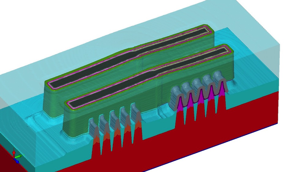
Figure 1 Bulk finFET (Source: Coventor)
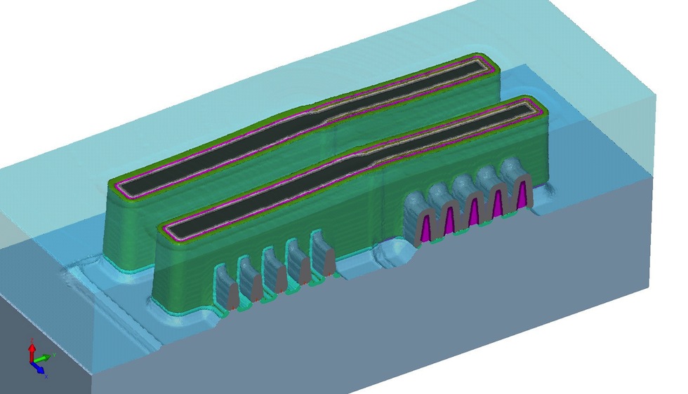
Figure 2 SOI finFET (Source: Coventor)
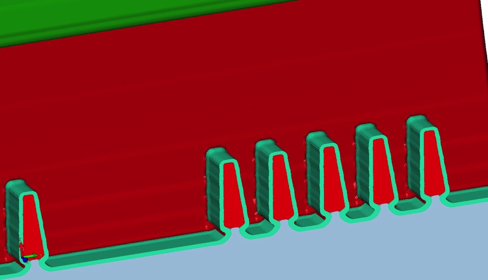
Figure 3 SOI FinFET mid-process showing overetch into buried oxide, which could lead to release of the fins, and subsequent defectivity. (Source: Coventor)
Fin thickness control
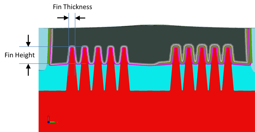
Figure 4 Cross section through the transistor gate showing the specific measurements of the fin, for transistor parametrics. (Source: Coventor)
FinFETs toy with fully depleted operation. If the fin is undoped, the transistor will operate in the fully depleted regime. The advantage of an undoped, fully depleted transistor is that the likelihood of transistor performance variations due to random dopant fluctuation is reduced. But, a fully depleted double-gate device’s threshold voltage is especially sensitive to body thickness (which in a finFET translates to the fin thickness). This problem is slightly reduced with increased fin doping, although this means sacrificing some of the intrinsic device advantages of a finFET. In any event, controlling the fin thickness variation is critical for controlling device variation. Making this even more challenging, fins are typically patterned using a sub-lithographic patterning scheme, such as sidewall image transfer, in order to meet the density targets of advanced nodes. These sub-lithographic schemes, challenging enough in their own right, will now be saddled with the extreme control regimes necessary to meet fin thickness variation objectives.
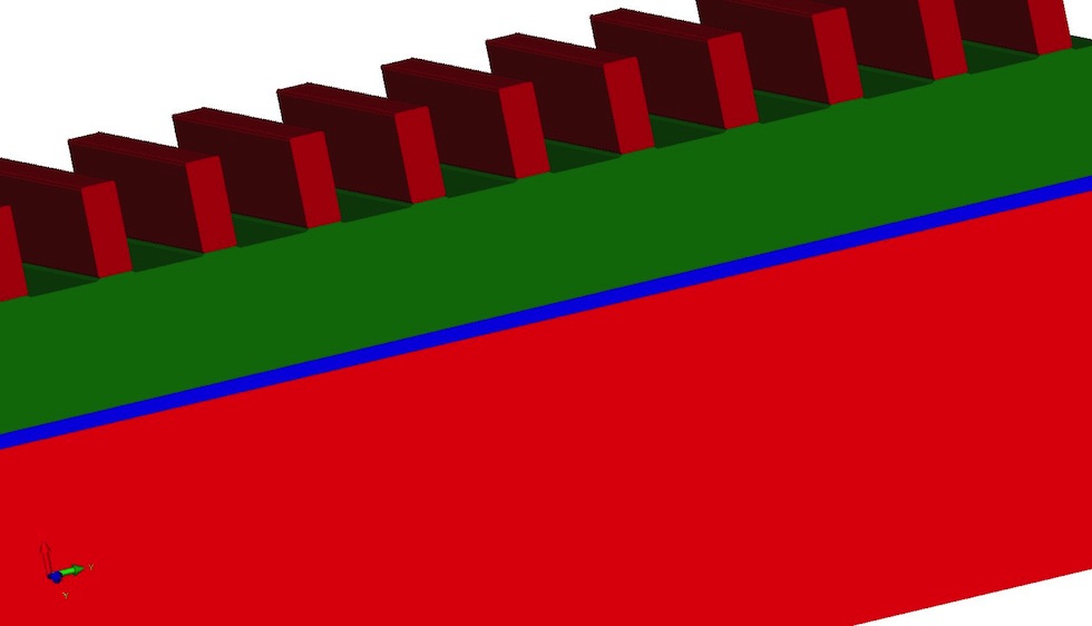
Figure 5 Process sequence showing sidewall image transfer where first, a mandrel is patterned at the lithographic limit (Source: Coventor)
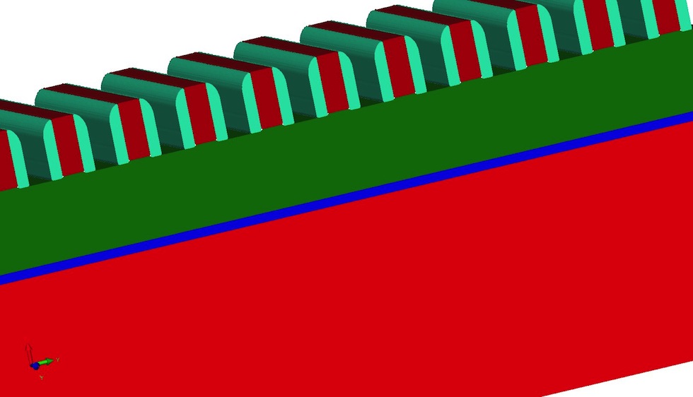
Figure 6 ...a spacer is added... (Source: Coventor)
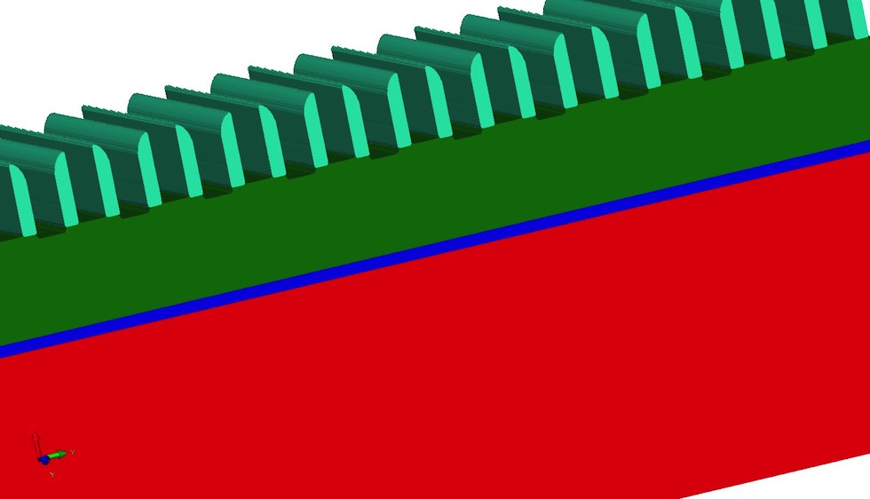
Figure 7 ...the mandrels are removed... (Source: Coventor)
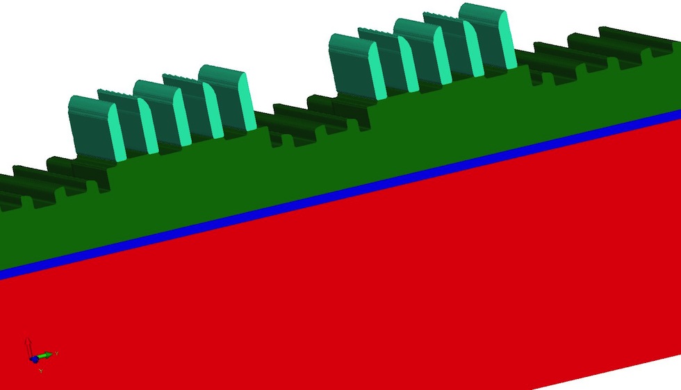
Figure 8 ...unwanted spacers are etched away and... (Source: Coventor)
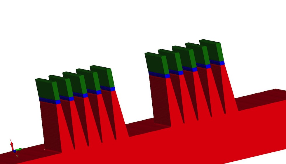
Figure 9 ...fins are etched with the spacers acting as a hardmask (Source: Coventor)
Density limitations in finFETs
No one wants finFETs to be a one-generation device, so the question is, “how scalable are finFETs to future technology nodes?” The answer is that the geometric scaling challenges are somewhat more complex in a finFET than historical planar nodes.
In one orientation, the fin pitch is limited by the sub-lithographic patterning scheme already described. Since the effective electrical width of one finFET is twice its height (give or take), the current density can be increased by either, making the fins at a tighter pitch or taller. Making the fins taller stresses the fin-patterning processes (in terms of variation control) and the subsequent process modules (gate definition, contacts, etc.), so device architects need to balance fin height and fin pitch. Any change to fin height or pitch will also have dramatic effects on the integration of all other process modules (especially the gate-metal fill processes), so scaling these dimensions to the next node will not be trivial.
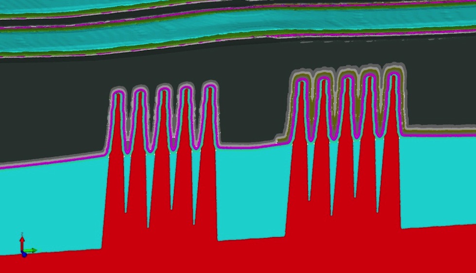
Figure 10 Example of a FinFET technology scaled to 14nm, requiring changes to the fin and metal-gate fabrication processes (Source: Coventor)
In the other orientation, the gate length will be limited by the gate patterning/integration and off-state leakage requirements, while the gate pitch will be predominantly limited by the source/drain architecture. The gate electrode is already double-patterned in most advanced nodes for pattern fidelity. While the introduction of EUV lithography will simplify this step significantly, fabs may have to use triple-patterning techniques in subsequent process generations until EUV is ready. Most advanced technologies are moving to replacement metal-gate techniques, and our ability to fill the gate trench with the proper metals is being tested. FinFETs make these processes more challenging than in planar technology, due to the requirements for film deposition on the near-vertical sidewalls of the fins.
The real challenge in this orientation comes from the source/drain architecture. Multi-fin transistors require the source/drain regions to either be merged (presumably with stressor epitaxy to gain performance), or electrically strapped (presumably with MOL metallization). The complex processes involved in integrating an effective source/drain (which will be different for NMOS and PMOS) and electrically contacting them will become the pinch-point for gate pitch scaling. The various source/drain architectures shown at IEDM will undoubtedly come under serious scrutiny for scalability.
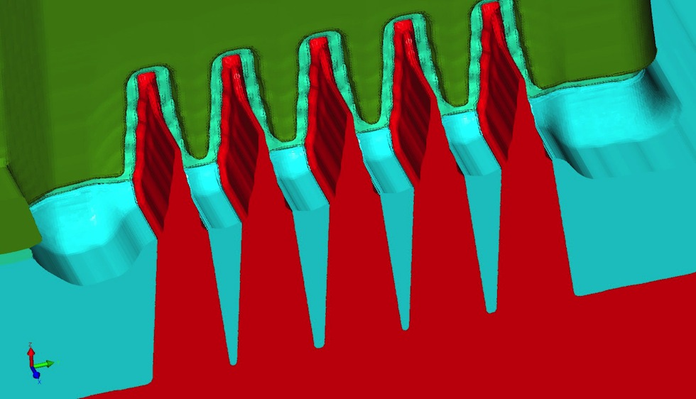
Figure 11 3D image mid-process before source/drain epitaxy showing unmerged fins (Source: Coventor)
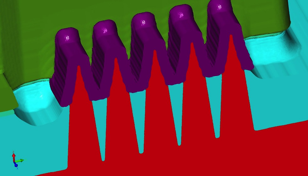
Figure 12 3D image mid-process after source/drain epitaxy, showing merged fins (Source: Coventor)
Those pesky ‘other’ devices
It’s often forgotten that most semiconductor products require more than just logic NMOS and PMOS transistors. Analog devices and passive elements, such as precision resistors, decoupling capacitors and ESD diodes, must also be fabricated alongside the advanced transistors. Fins are inherently narrow, and therefore present current-carrying limitations for many of these ‘other’ devices. As such, many proposed finFET technologies integrate these analog elements with larger planar regions, requiring some additional, and perhaps even divergent, processing. When you restrict the suite of devices offered on a process it has inevitable implications for product design, but this is what we expect to see in finFET technologies. The choice of devices to integrate alongside fins, and the additional planar processes necessary to build them, will be a key part of defining the device-menu and total process complexity.
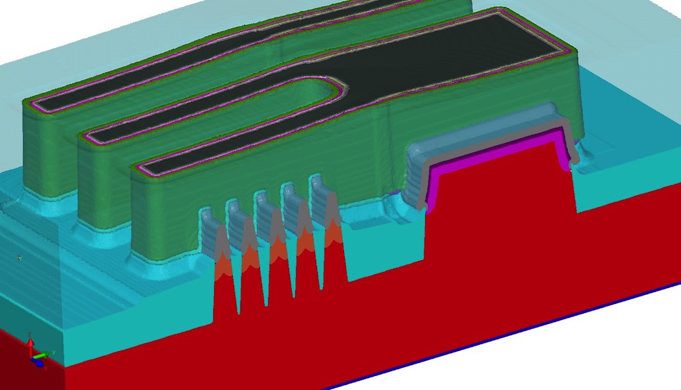
Figure 13 3D Image showing FinFET transistors integrated with wide planar device for analog or passive applications (Source: Coventor)
Process complexity in bulk finFETs
It’s getting increasingly complex to make these devices, which affects the overall likelihood of process variability affecting device performance. Here’s an animated simulation of the steps required to build a finFET on bulk:

Figure 13 Building a bulk finFET, step by step (Source: Coventor)
Process complexity in SOI finFETs
For completeness, here’s a similar animation for SOI finFETs
Figure 14 Building an SOI finFET, step by step (Source: Coventor)
Conclusion
As with any other technological paradigm shift, finFETs are not simple. There are many ways to build them and solve the complex issues involved in doing so. Decisions on these solutions will dictate the process complexity and therefore the cost, manufacturability and eventual success of finFET technologies in the marketplace.
The 3D models used in this work were produced by Coventor’s SEMulator3D platform, which builds high-resolution predictive 3D models of semiconductor devices, based on a parametrized process description and any applicable design data. Virtual metrology and batch execution capabilities enable thorough investigation of process variation and allow process changes to be validated across the design space. SEMulator3D is used to solve complex semiconductor design-technology challenges at major foundries, IDMs, equipment suppliers and fabless semiconductor companies.
Author
Dr David M Fried is chief technology officer – semiconductors at Coventor, responsible for the company’s strategic direction and implementation of its SEMulator3D modelling platform. His expertise touches upon such areas as silicon-on-insulator (SOI), FinFETs, memory scaling, strained silicon, and process variability. Fried holds 45 patents and spent 14 years at IBM, most recently as 22nm Chief Technologist for IBM’s Systems and Technology Group. He has Masters and Doctoral degrees in electrical engineering from Cornell University.
Company
4000 Centregreen Way, suite 190Cary, NC, 27513
Phone: (919) 854-7500 x 132
Fax: (919) 854-7501
