Synopsys FPGA prototyping launch puts pragmatism first
FPGA prototyping has been very busy this year. Things show little sign of letting up with Synopsys’ launch of its HAPS-70 series boards.
The highlights:
- The boards feature the latest Xilinx Virtex-7 devices.
- They can scale from 12 million ASIC gates equivalent to 144 million (from 1 x Virtex, through to 12 x Virtex delivered in 3 x 4-chip modules).
- Inter-FPGA communication gets a turbo-charge from the use of high-speed time-domain multiplexing (HSDTM).
- Debug visibility is raised by a move to an off-FPGA memory module, allowing, Synopsys says, a 100X increase in trace storage.
- Synopsys’ Certify FPGA prototyping software has had another tweak to speed and ease logic partitioning.
Two things caught our attention.
Divide to conquer FPGA prototyping
First, let’s take the scaleable model and the HSDTM capability together. The boards come in combinations of 1-, 2- and 4-chip modules that can be assembled in up to three modules. That let’s you build capacity for a very complex design. But product marketing manager Neil Songcuan explained it also addresses designs with multiple IP blocks that you have prototyped separately or want to keep separate (perhaps for ease of partitioning).
IP proliferation on even an entry-level smartphone design is serious. Modularity helps you knit together processor cores, MIPIs, HDMIs, and so on in a pragmatic way. But for FPGA prototyping, even if you split the IPs and other custom portions over multiple devices, they must talk to one another and the heart of your design at speeds approaching those expected from final silicon. A prime FPGA prototyping use-case remains evaluation in real-world conditions.
That’s where the HSDTM move comes in. To that end, Synopsys has produced this table showing what it sees as the potential boosts in inter-FPGA performance.
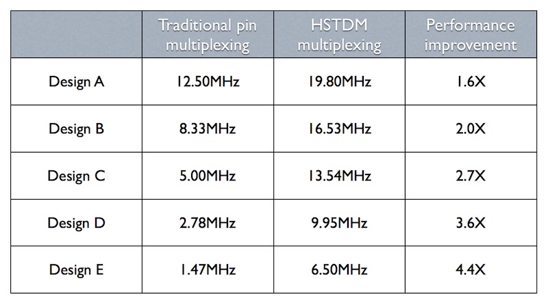
Figure 1
Traditional pin vs high-speed time-domain multiplexing for FPGA prototyping (Source: Synopsys – click image to enlarge)
The nice thing about these enhancements is that you can see how they fit together from a common sense point-of-view. There’s a divide-and-conquer option here (and it has echoes of Synopsys parallel work on hybrids that leverage both virtual and FPGA prototyping).
The debug crunch in FPGA prototyping
Second is the decision to increase debug capacity by going off-FPGA. As complexity drives up the need for debug traces, so the greater utilization of FPGA prototyping capacity is reducing the capacity available to do that on the array(s) in-use. Synopsys estimates about 10% capacity, but I’ve seen lower quoted.
It’s just over a week since Tektronix came up with a novel approach based on making highly efficient use of on-FPGA capacity with smart compression algorithms. The Synopsys response of adding external memory storage may feel a little low-tech in comparison, but can still lay claim to a 100X increase in available traces. Ultimately, you makes your choice and you pays your money (the cost comparison on the two solutions will be interesting). This is one that the market now gets to decide.
After all that, not going into too much detail on the productivity boosts in Certify might seem a bit strange. But those are more on the ‘expected’, even ‘required’ side, and you can find more about those enhancements online. What’s more interesting about HAPS-70 are the daily design challenges it responds to.
